Returning Customer
I am a returning customer
Register Account
If you already have an account with us, please login at the login form.
Your Account Has Been Created!
Congratulations! Your new account has been successfully created!
You can now take advantage of member privileges to enhance your online shopping experience with us.
If you have ANY questions about the operation of this online shop, please e-mail the store owner.
A confirmation has been sent to the provided e-mail address. If you have not received it within the hour, please contact us.
Account Logout
You have been logged off your account. It is now safe to leave the computer.
Your shopping cart has been saved, the items inside it will be restored whenever you log back into your account.
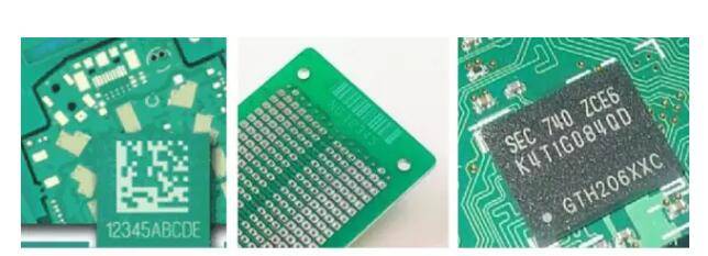
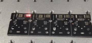
PCB board, in short, the circuit board, is the provider of electrical connections for electronic components. Almost all electronic products will use the PCB board, such as mobile phones, computers, multimeters and other electronic products. With the increasingly complex varieties and batches of PCB board products, businesses increasingly face difficulties in product management. In order to achieve the quality control in the PCB production process, the characters, bar codes and QR codes are printed on the PCB board to trace the information and become the booster of industrial innovation and development.
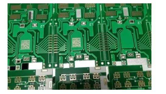
Screen printing marking method
Screen printing process is to use the production of a good graphic screen, under the pressure of character ink from the screen part of the mesh through and leak printed on the surface of the circuit board, and the rest of the screen mesh will be Being blocked, can not through the ink, only the surface of the circuit board to form a blank, thus forming words, logos, patterns.
advantage
The initial investment cost is relatively low, marking speed
Disadvantages
Easy to fall off: The ink on the surface of PCB board is easy to fall off due to friction during use, fading, causing the characters to be blurred.
Easy to remove: hydrochloric acid or cyclohexanone solution can be directly removed from the surface of the PCB characters, easily lead to information tampering.
Consumables: Screen printing needs to continue to consume ink and other accessories tools.
Rough information: Screen printing can only be marked on a larger PCB board, and the font is rough and unclear.
Pollution of the environment: organic solvents used in the printing process and heavy metal elements such as chemical raw materials, has a certain toxicity, will cause personal injury to workers, and pollute the air and the environment.
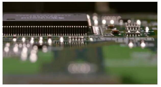
Laser marking marking method
Laser marking is the use of high-energy density laser PCB on the local irradiation, the surface layer material vaporization or color changes in the chemical reaction, leaving a permanent marking a marking method. Laser marking can play a variety of text, symbols and patterns, the character size can range from millimeters to microns, which is of special significance for the security products
advantage
Anti-damage: the use of laser etching directly on the surface of the text, symbols, permanent, able to resist damage.
Easy to operate: Simply design your graphics on your computer to make the graphics appear instantly.
Marking clear: high precision laser processing, spot fine, fine marking can be achieved, the pattern clear and beautiful.
Save material: "non-contact" processing does not damage the workpiece, does not destroy the material, save material costs.
Safety and Environmental Protection: Only a small amount of gas is generated and exhausted through exhaust gas. There is no need for chemical substances to help protect the safety and working environment of the operator as much as possible.
Low operating costs: laser marking consumes only a small amount of electricity, without ink and other accessories.
Disadvantages
The initial investment cost is relatively high
With the rapid development of electronic product manufacturing technology, portable electronic products are increasingly becoming more and more miniaturized, highly integrated and lightweight. Combined with the development of packaging technology, pads and spacing smaller and smaller, making the printing alignment has become more difficult. The laser marking its accuracy and flexibility to overcome the easy-off screen printing, processing accuracy is not high and other technical shortcomings in the PCB industry will play a decisive role!